Two Phase Traffic Diversion System
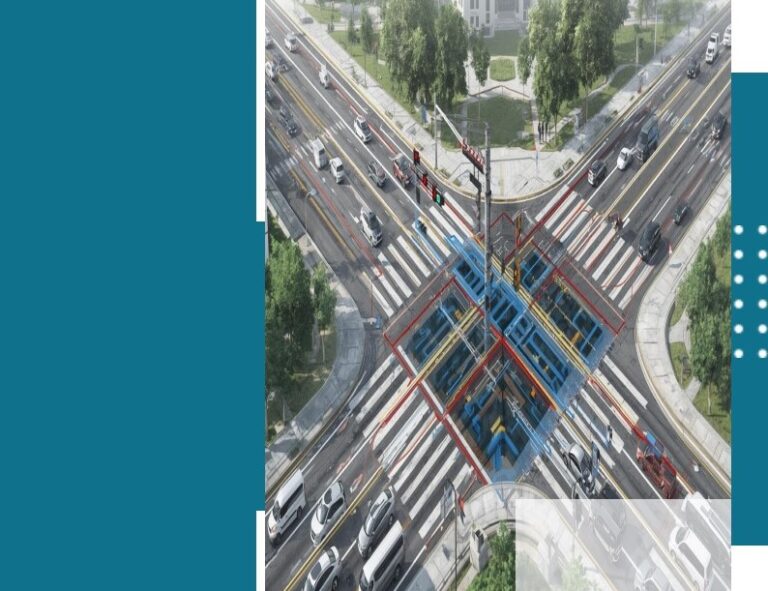
Technical Description This invention discloses a traffic diversion signaling system that converts a conventional four phase intersection into a simplified two phase scheme using straight through, stop, and custom “C / inverse C” signals. By prohibiting direct right (or left)…