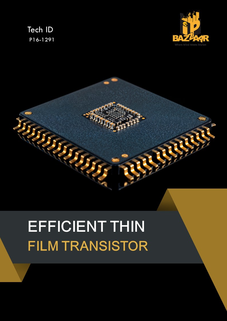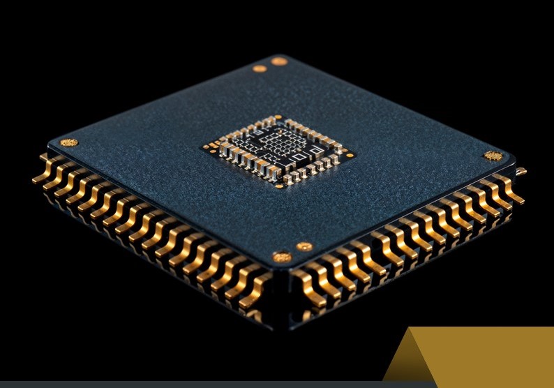
Technical Description
This invention introduces a thin film transistor with an optimized gate interface, enabling low operating voltage, enhanced electron mobility, and reduced trapping density for improved performance.
Problems Addressed
- High Operating Voltage
- Excessive Gate Leakage
- Limited Electron Mobility
- High Interface Trap Density
- Restricted Low-Power Applications
Tech Features
- Enhanced Electron Mobility
- Low Operating Voltage
- Optimized Subthreshold Swing
- Reduced Interface Trap Density
- Advanced Material Selection
- Optimized Process Integration
Target Audience
- Electronics Manufacturers
- Semiconductor Industry
- Industrial & Medical Equipment Maker
- Research and development Institution
Tech ID: P16-1291 TRL 4 Patent Status: Granted Available For Exclusive and Non-exclusive License